25+ successive approximation adc block diagram
A DAC on the other hand inputs a binary number and outputs an analog voltage or current signal. The functional block diagram of successive approximation type of ADC is shown below.
Analog To Digital Converter Block Diagram Types Its Applications
Analog to Digital Converters.
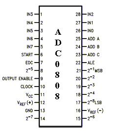
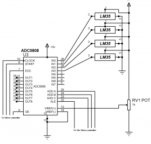
. Consider using a binary counter as the input to the DAC that. ADC0808 Description The ADC0808 IC is a typical ADC module for projects that require an external ADC. Each channel can be sampled with a different sampling time.
The logic diagram for the same is shown below. 由於是Successive Approximation ADC 所以有n bits就需要n的cycle來迭代可參考上面的Successive Approximation ADC說明. ATMega microcontrollers contain multi-channel Analog to Digital Converter ADC subsystemThe ADC has 10-bit resolution and works on the principle of successive approximation.
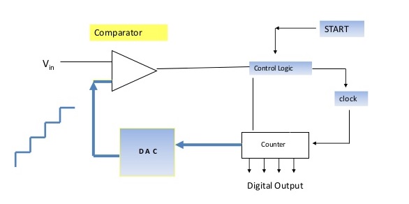
The successive approximation ADC mainly consists of 5 blocks Clock signal generator Successive Approximation Register SAR DAC comparator and Control logic. The AM335x microprocessor contains the subsystems shown in the Functional Block Diagram and a brief description of each follows. Core block diagram and operating modes.
The conversion time is a function of the conversion clock frequency and the resolution of the ADC. 512B RAM MSP430BT5190 25 MHz MCU with 256KB Flash 16KB SRAM 12-bit ADC Commercially Licensed Bluetooth v21 Stack MSP430F1101. It always takes the same amount of time.
The successive approximation register provides the digital code to the internal DAC during each conversion clock cycle. The AM335x microprocessor contains the subsystems shown in the Functional Block Diagram and a brief description of each follows. The block diagram of ADC is shown below which includes sample hold quantize and encoder.
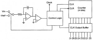
Functional block diagram ad7682ad7689 ref gnd vdd vio din sck sdo cnv 18v to vdd 23v to 55v sequencer spi serial interface mux 16-bit sar adc band gap ref temp sensor refin in0 in1 in4 in5 in6 in7 in3 in2 com 05v to vdd 10µf one-pole lpf 05v to vdd 05v 01µf 07353-001 figure 1. A successive-approximation ADC is a type of analog-to-digital converter that converts a continuous analog waveform into a discrete digital representation using. The architecture is based on capacitive redistribution which inherently includes a sample-and-hold function.
12-Bit Successive Approximation Register SAR ADC. Delta-sigma modulation is inspired by delta modulation as shown in Figure 2If quantization were homogeneous eg if it were linear the following would be a sufficient derivation of the equivalence. Starting with the MSB are 25 125 0625 03125 015625 0078125 00390625 001953125 0.
Start with a block diagram of a delta modulatordemodulator. The converter is fabricated on a 06μm CMOS process. It is associated with three registers ADC Multiplexer Selection Register ADC Control and Status Register and ADC Data Register.
25 ppmC REFERENCE INPUTOUTPUT Reference Input Voltage Range See the ADC Transfer Function section 2495. SAR ADC SERIAL INTERFACE VIO REF VDD VREF 0 VREF2 HIGH-Z MODE CLAMP SPAN COMPRESSION TURBO MODE STATUS BITS 24V TO 51V 18V 10µF 18V TO 5V 3-WIRE OR 4-WIRE SPI INTERFACE DAISY CHAIN CS 14956-001 Figure 1. ADC Successive Approximation 8-Bit 1 Func 1 Channel Parallel 8 Bits Access CMOS PDIP20 ComSIT.
Enter the email address you signed up with and well email you a reset link. GENERAL DESCRIPTION The AD4000AD4004AD4008 are high accuracy high speed low power 16-bit Easy Drive. The XPT2046 is a classic successive approximation register SAR analog-to-digital converter ADC.
Europe - USA - Asia Single ADC SAR 10ksps 8-bit Parallel 20-Pin PDIP Rail. 18-Bit 15Msps SAR ADC X LTC2387-18 The LTC2387-18 is a low noise high speed 18-bit 15Msps successive approximation register SAR ADC ideally suited for a wide range of applications. The final output DAC voltage is 25 0625 03125 34375V The advantage of the successive approximation ADC is that it is deterministic ie.
It consists of a successive approximation register SAR DAC and comparator. An analog to digital converter ADC AD or A to D is a device that converts a continuous physical quantity usually voltage to a digital number that represents the quantitys amplitudeIn block diagram form it can be represented as such. 1-ch 12-bit successive approximation adc serialparallel access pqcc28 rohs compliant plastic mo-047ab lcc-28.
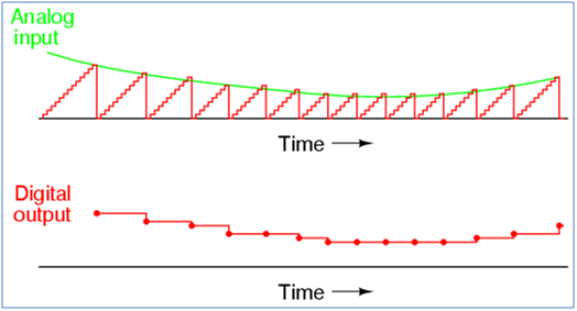
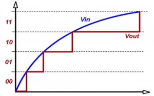
Successive-approximation ADC block diagram showing digital-to-analog converter. Step size is the change in analog input to cause a unit change in the output of ADC. Sample Time 3 - 480 cycles.
General description the ad7682ad7689 are 4-channel8. The device features a 4 -channel 12-bit successive approximation register SAR ADC eight 12-bit DACs four bipolar and four unipolar with output ranges that can be configured to shut down under external pin control a 125C accurate internal temperature sensor and eight general-purpose inputoutput GPIO pins. Figure 2d and Extended Data Fig.
December 24 2019 at 125 PM For me the PWM output values change from 0 1024 as expected but the pot moves only till half so i divided the ADC by half to match the. 12-Bit Successive Approximation Register SAR ADC. CCPR1L 00 duty-500100 duty and it worked Except when the ADC is above 1000.
The working of a successive approximation ADC is as follows. Hence it is called a s dual slope A to D converter. ADCCLK cycles that can be modified using the SMP20 bits in the ADC_SMPR1 and ADC_SMPR2 registers.
512B RAM MSP430BT5190 25 MHz MCU with 256KB Flash 16KB SRAM 12-bit ADC Commercially Licensed Bluetooth v21 Stack. 2 1 MSPS. The step size is chosen dependent upon the set reference value.
FUNCTIONAL BLOCK DIAGRAM. In the simplified 5-bit SAR ADC example above the 5 conversion clock cycles are required to reach the end of the conversion. The block diagram of a successive approximation ADC is shown in the following figure.
The linearity property of integration makes it possible to move the integrator which reconstructs the analog. Successive Approximation AD Converter by electronicsdit. To support versatile MVM directions most of the design is symmetrical in.
Successive Approximation ADC Block Diagram Flash Type ADC Direct. 1-CH 16-BIT SUCCESSIVE APPROXIMATION ADC SERIALPARALLEL ACCESS QCC48 MO-220VKKD LFCSP-48. In dual slope type ADC the integrator generates two different ramps one with the known analog input voltage VA and another with a known reference voltage Vref.
The equivalent analog output voltage of DAC VD is applied to the non-inverting input of the comparator. The basic operation of the XPT2046 is shown in Figure 4. Dual 16-bit successive approximation register SAR ADC.
The output of SAR is given to n-bit DAC. 1 show the block diagram of a single CIM core.
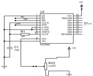
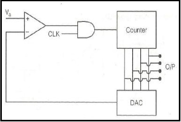
Counter Type Adc Working And Its Advantages And Disadvantages
Analog To Digital Converter Block Diagram Types Its Applications

Ad584 Precision Voltage Reference Datasheet Pdf Download

Analog To Digital Conversion Adc Analog To Digital Converter Block Diagram Digital
Analog To Digital Converter Block Diagram Types Its Applications
Analog To Digital Converter Block Diagram Types Its Applications

Ad584 Precision Voltage Reference Datasheet Pdf Download
Counter Type Adc Working And Its Advantages And Disadvantages
Analog To Digital Converter Block Diagram Types Its Applications
2
Counter Type Adc Working And Its Advantages And Disadvantages
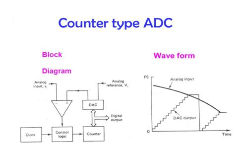
Counter Type Adc Working And Its Advantages And Disadvantages
Analog To Digital Converter Block Diagram Types Its Applications

Ad584 Precision Voltage Reference Datasheet Pdf Download

Analog To Digital Conversion Adc Analog To Digital Converter Circuit Diagram Digital
Analog To Digital Converter Block Diagram Types Its Applications
2